Under Bump Metallization (UBM) is required for connecting the die to the substrate with solder bumps for Flip-Chip packages. The UBM of the integrated circuit (IC) bonds pads that are typically aluminum but can be copper. This is an essential process step for the reliability of the electronic package.
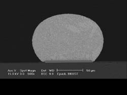
Example of solder bump plated onto underbump metallized surface.
As with most processes, several options are available to achieve Under Bump Metallization (UBM). The dry vacuum sputter method combined with electroplating is the most common method used consisting of multi-metal layers sputtered in a high temperature evaporation system. Although the dry vacuum sputter process is the benchmark and the most readily used, other alternatives have been introduced and are quickly establishing their place in the market due to the cost and throughput limitations experienced with the dry vacuum sputter process.
Regardless of the UBM method utilized, the final layer of many IC bond pads typically consists of aluminum, aluminum/silicon, aluminum/silicon/copper or copper. Aluminum is suitable for conventional wire bonding interconnects since the wire bonding techniques form acceptable connections through the oxide layer normally present. But, aluminum is not solderable, wettable or bondable to the bump and soldering materials used in reflow. The UBM layer produces a good bond to the aluminum pad, hermetically seals the aluminum, and prevents the potential of diffusion of metals into the IC package. UBM is necessary for successful flip chip and solder bump interconnected packages.
A quickly emerging alternative for UBM is Electroless Nickel/Immersion Gold (ENIG). Unlike the dry vacuum sputter process, this technology consists of wet chemical processes that offer economic and throughput advantages. The dry vacuum sputter process requires large capital costs for equipment with relatively low yields. One advantage experienced with the wet chemical process includes one tool that can be sized to produce several wafers at a time while processing in cassette trays. The tool is typically automatic, and if required, can process up to several hundred wafers per shift. The ENIG UBM process is being established at companies that are cost-sensitive and where high-volume production is required.
Aluminum Oxidizes Quickly
Aluminum forms oxides almost immediately when it is exposed and not protected from the environment. Because of that, the first challenge in UBM processing is to remove the oxidation layer from the aluminum IC pad. The aluminum oxide can be removed by sputter etching, ion etching, or with a wet chemical treatment.
As with any wet chemistry deposition, the quality of the finish is only as good as the surface that is being plated. The surface preparation is a critical portion of the UBM plating process. The aluminum preparation must be fine-tuned according to the material type or blend being plated. Different aluminum surfaces always require adjustments in time, temperature, or process concentrations. Copper IC pads require a completely different pretreatment and activation process, which is covered later in this discussion.
Pretreatment for Aluminum
Cleaner. The cleaner removes any contamination from the surface prior to chemical treatment. It also wets the surface to enhance solution transfer. Typically wafer surfaces are free of handling oils or fingerprints, so the cleaner primarily ensures that the surface is wetted.
Etching. The micro-etching process removes or minimizes the aluminum surface oxide layer. The micro-etch bath prepares the surface for the subsequent thin nitric acid oxide layer. The aluminum alloys and pad thickness dictates the operating conditions of the micro-etch bath.
First Nitric Acid Dip. The nitric bath forms a thin uniform oxide layer on the aluminum IC pad. The thin oxide layer improves the uniformity of the subsequent zincate coating while leaving a relatively pure aluminum surface by dissolving alloying constituents.
First Zincate. The first zincate bath dissolves the aluminum oxide on the surface and deposits zinc through a galvanic reaction that takes place. The zinc coating protects aluminum from air re-oxidation and also seeds the aluminum for the electroless nickel plate that comes later.
Second Nitric Acid Dip. When the base aluminum is greater then 0.5µ thick the initial zincate coating is stripped off and a second uniform thin oxide coating is formed on the aluminum.
Second Zincate. A second zincate layer is used because of the superior zinc deposit uniformity when compared to the first zincate step by itself. It is essential that the underlying aluminum is not excessively attacked during the nitric acid dips and zincate process.
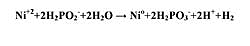
Electroless Nickel. The electroless nickel is an autocatalytic (electrochemical mechanism, both oxidation and reduction) process that uses a reducing agent. The reducing agent, hypophosphate (H2PO2), is typically used. The chemical deposition of nickel metal by hypophosphite meets both the oxidation and reduction reaction potential criteria. The enclosed chemical equation simplifies the reaction that takes place (Formula 1):
The nickel layer forms an adherent coating to the IC and acts as a diffusion barrier to protect the IC. Nickel provides a solderable surface for the bump application, and an aluminum wire bondable surface.
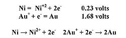
The nickel thickness deposited depends on the end use application; typically a minimum of two microns is used for UBM applications. Immersion Gold. Immersion gold plating onto nickel is a displacement reaction; no reducing agent is required. Displacement reactions take place when a more noble metal ion in solution is displaced from its ionic state by a less noble substrate. The simplified reaction is (Formula 2):
The immersion gold target thickness is typically around two micro inches. A thin gold coating prevents the nickel from passivating, thereby maintaining solderability. In a soldering application, gold dissolves into the solder and the intermetallic bond formed is nickel/tin. Tight control of the immersion gold process inhibits the gold chemistry from excessively corroding the underlying nickel. Nickel that is excessively corroded will compromise the solderability of the IC.
Pretreatment for Copper
Cleaner. The cleaner removes soils and contamination from the surface prior to chemical treatment. It also wets the surface, which will enhance solution transfer.
Micro-etch. The micro-etching process removes copper surface oxide. The micro-etch bath roughens the copper, which enhances the adhesion of the nickel.
Acid rinse. The acid rinse ensures that the copper surface is oxide-free and any residual copper has been removed.
Pre-dip. The pre-dip minimizes the acid dilution of the of the subsequent activator bath.
Activator. The Activator is an immersion reaction bath that displaces copper and seeds it with palladium. The palladium initiates the subsequent autocatalytic nickel plating step. Electroless Nickel. The electroless nickel is an autocatalytic process. The nickel layer acts as a diffusion barrier that is solderable or aluminum wire bondable.
Immersion Gold. The immersion gold plating is a displacement reaction. The thin gold coating maintains long-term solderability and prevents the nickel from oxidizing and passivating.
Gold Wire Bonding
Some specific applications require gold wire bonding to IC pads. In order to do this, three options are available: Gold Sputtering, Electroless Gold, and Electroless Palladium.
Gold Sputtering. The dry vacuum sputter process can be used to add more gold onto the IC pads to make them suitable for the gold wire bonding process. The additional gold being sputtered can range from 1 to 2µ in thickness. Although the dry sputtering process can be utilized in the production process, its high cost and time required have made other alternatives more attractive.
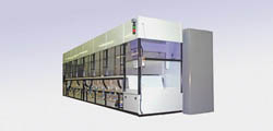
A bump line made by Precision Process Equipment, Inc., Niagara Falls, NY.
Electroless Gold (Electroless Ni/Immersion Au/Electroless Au). Electroless gold plating solutions that are typically used are neutral pH, autocatalytic baths. The reducing agents employed are proprietary. Electroless gold is deposited onto the IC pads over the thin immersion gold layer that is plated over the electroless nickel. The complete process is done in one stage with multiple wafers processed at the same time in cassette trays, making this process attractive to high-volume users. The target gold thickness is typically in the 20 microinch range.
Electroless Palladium (Electroless Nickel/Electroless Pd/Immersion Au). Using Electroless Nickel/Electroless Palladium/Immersion Gold (ENEPIG) process for gold wire bonding is yet another option that is becoming popular. The ENEPIG surface finish provides both a solderable surface and a gold or aluminum wire-bondable IC pad. The electroless Pd is typically in the 2 to 6 microinch range topped with the immersion gold being plated in the 1 to 2 microinch range. The lower precious metal thickness and cost provides a more cost-effective alternative relative to other available options. This complete process can also be done in one tool with multiple wafers at a time while processing in cassette trays, thus eliminating any productivity concerns.
In UBM several options are available in today's market. Wet chemical UBM is an option to consider for its benefits of production throughput and lower cost. Several different chemical processes are commercially available to choose from. They are Electroless Nickel over Al or Cu, Electroless Ni/Immersion Au or Electroless Ni/Immersion Au/Electroless Au for soldering and wire bonding applications. Lastly, Electroless Ni/Electroless Pd/Immersion Au provide a less costly alternative to electroless Au.
It's important to choose the correct process that meets all the end use requirements. The pretreatment must be optimized for the specific substrate being produced in order to achieve the optimum results. So, if you are setting up a new UBM process or looking at increasing productivity and reducing costs, look around, since several proven production options exist.
Go to under bump metallization page – aluminum
Go to under bump metallization page – copper
Go to under bump metallization page – CMOS-compatible